|
JeVois
1.23
JeVois Smart Embedded Machine Vision Toolkit
|
|
|
JeVois
1.23
JeVois Smart Embedded Machine Vision Toolkit
|
|
This connector (located between the two USB ports at the top of the camera, see Overview of the JeVois-Pro hardware platform) provides power to auxilliary gadgets you may want to connect to JeVois-Pro. This power is derived from the main 6-24VDC barrel jack input of JeVois-Pro.
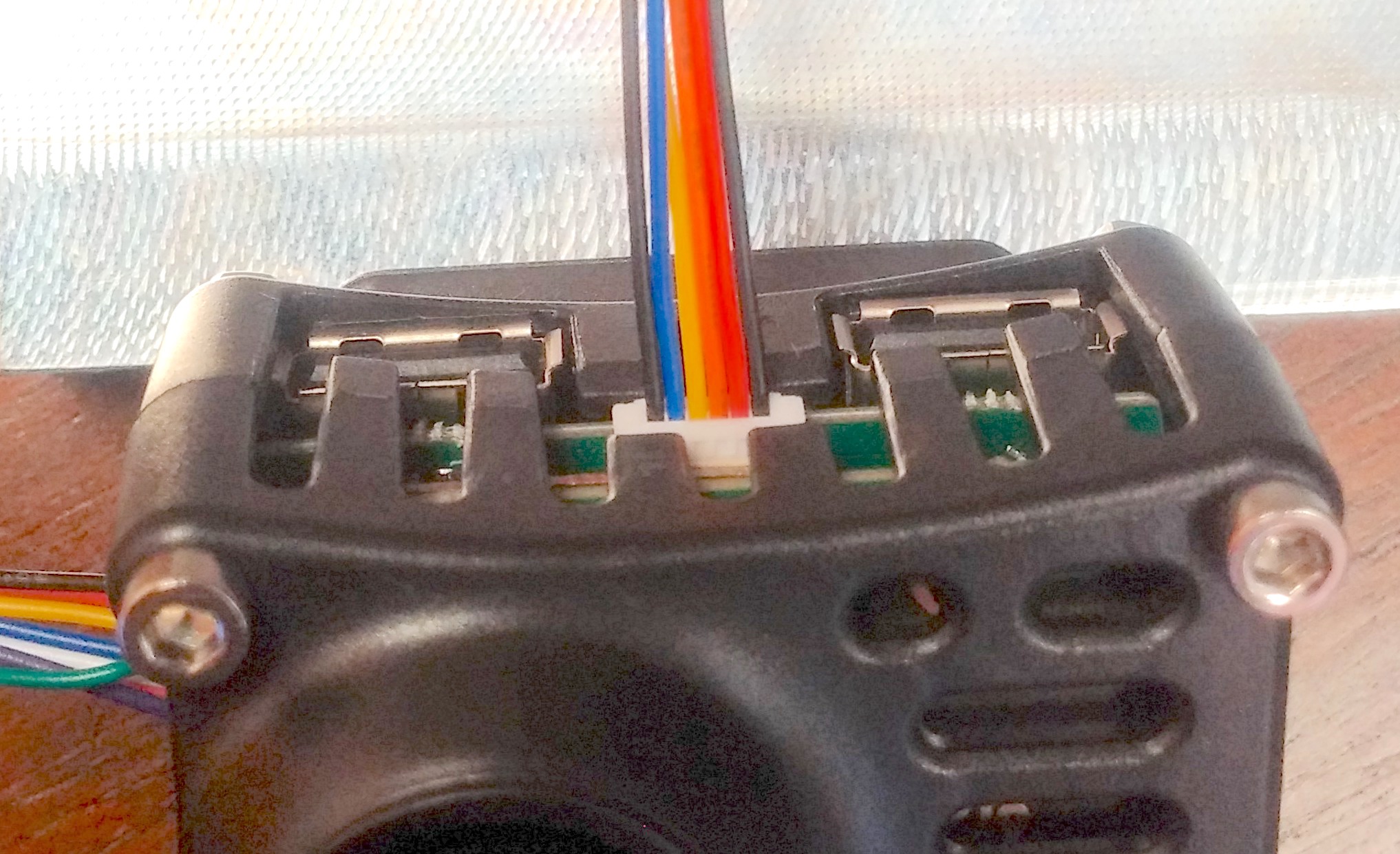
Note the connector orientation and the order of the colored wires above.
The pinout is as follows:
| Pin | Wire color | Function |
|---|---|---|
| 1 | Black | GND |
| 2 | Red | 5V / 1A (shared with USB host 1, connector at left when looking from behind JeVois-Pro) |
| 3 | Orange | 5V / 1A (shared with USB host 2, connector at right when looking from behind JeVois-Pro) |
| 4 | Yellow | 3.3V / 750mA |
| 5 | Blue | 1.8V / 500mA |
| 6 | Black | GND |
Mating connector part number: JST SHR-06V-S-B which is 1.0mm pitch, 6-pin JST-SH series.
The pins for these connectors are almost impossible to crimp by hand, unless you have the special $1000+ tool sold by JST. Thus, please take good care of the cable that was provided with your JeVois-Pro camera. Extend the wires instead of cutting them very short...
Note that the current rating of each pin of this connector is 1A. Since there are only two GND pins, try to not draw more than 2A over the other 4 pins combined.
This connector (located next to the micro-HDMI connector, see Overview of the JeVois-Pro hardware platform) provides 6 general input/output pins (GPIO). The pins can be configured in various ways, as detailed below.
Like with the 4-pin serial port, this port expects an input voltage to be provided on pin 6 (IOREF). This is an input to JeVois-Pro that your must provide to tell JeVois-Pro the voltage level that you want the GPIO pins to operate at: 3.3V or 5V. See Serial port user guide for more info.
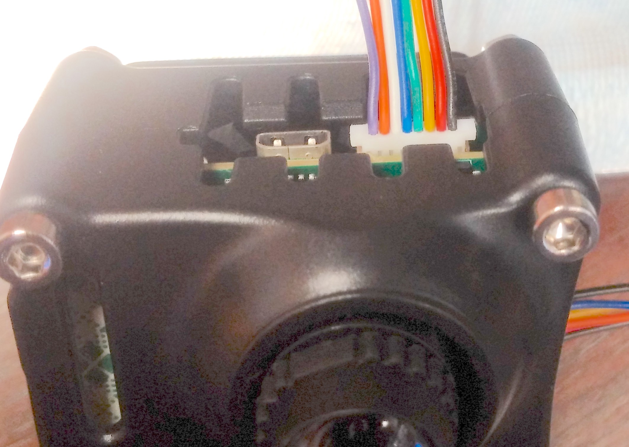
Note the connector orientation and the order of the colored wires above.
The pinout is as follows:
| Pin | Wire color | Function | A311D SoC | Kernel GPIO |
|---|---|---|---|---|
| 1 | Purple | JVGPIO0 / SPI MOSI / SPDIF_OUT / UART_RTS | GPIOH_4 | 431 |
| 2 | Orange | JVGPIO1 / SPI MISO / SPDIF_IN / UART_CTS / PWM_F | GPIOH_5 | 432 |
| 3 | White | JVGPIO2 / SPI SS / UART_RX / IR_OUT / ONEWIRE / ISO7816_CLK | GPIOH_6 | 433 |
| 4 | Blue | JVGPIO3 / SPI SCLK / UART_TX / ISO7816_DATA | GPIOH_7 | 434 |
| 5 | Green | JVGPIO4 / I2C SDA | GPIOZ_14 | 425 |
| 6 | Yellow | JVGPIO5 / I2C SCL | GPIOZ_15 | 426 |
| 7 | Red | IOREF (you provide voltage at which GPIOs operate: 3.3V or 5V) | - | - |
| 8 | Black | GND | - | - |
Mating connector part number: JST SHR-08V-S-B which is 1.0mm pitch, 8-pin JST-SH series.
The pins for these connectors are almost impossible to crimp by hand, unless you have the special $1000+ tool sold by JST. Thus, please take good care of the cable that was provided with your JeVois-Pro camera. Extend the wires instead of cutting them very short...
JVGPIO0 to JVGPIO3 are connected via a voltage level translator, an NXP NTB0104GU,115 chip. This chip automatically senses input or output direction. This is a great feature as we do not need an extra pin for each GPIO to indicate whether it currently is used as input or output and to set the translator's direction accordingly. But it comes with some caveats: If you are using a pin as output, but connect it to a device that could supply current, for example because there is a pull-up resistor on an input of your device, the NTB0104 chip could reverse its direction. Generally this will not destroy your hardware but it can lead to unexpected results.
For example, we tried to connect a Sparkfun ICM20948 external IMU to the GPIO connector of JeVois-Pro using the SPI bus. We could not make it work and would always read garbage from the device and could not see SPI transfers on the pins of the Sparkfun board using an oscilloscope. As it turns out, the Sparkfun board has its own set of voltage translators with some 2.2k pullup resistors on all pins. Likely this was enough for our NTB0104 to think that all pins from the Sparkfun board were outputs, and thus it configured itself as sending data from the Sparkfun board to the A311D of JeVois-Pro on all 4 SPI pins. This is a problem since MOSI, SS, and SCLK should actually send data from the A311D to the Sparkfun board. To fix this, you would likely need to insert some unidirectional buffers in front of that Sparkfun IMU (e.g., 74HC125 or similar with 3 buffers connected A311D->Sparkfun (MOSI, SS, SCLK) and one connected Sparkfun->A311D (MISO); note that we have not tried this yet but we will soon).
Because of the NBT0104, when used as inputs, JVGPIO0 to JVGPIO3 are also "sticky" as the NTB0104 will maintain the current drive state until it is actively changed. For example:
JVGPIO4 and JVGPIO5 use simple MOSFETS for voltage translation, with 2k pullup resistors to IOREF. When configured as inputs (see below), these pins will read "1" by default because of the pullups, unless you actively drive them to 0V (GND), in which case they will read "0".
For more information, check out the schematics in: Hardware: Schematics, case STL files, etc
To activate a given GPIO, look up its Kernel GPIO number from the last column of the above table, and issue these commands in a Linux shell as root (or in the JeVois Console, using shell as a prefix), replacing 431 below with the Kernel GPIO number you want to use:
For direction, you can also use low to set as output and immediately set the output level to low in a glich-free manner, or high to set as output and immediately set the output level to high glitch-free.
If you want to free up this GPIO after claiming it:
Example for JVGPIO0:
Example for JVGPIO0:
We may have made a mistake and used pullups that are too strong for the A311D to overcome. Or there might be specific issues because these pins have special OD (open-drain) drivers on the A311D but we could not find much about this in the A311D datasheet. While we try to figure this out, please use this hack:
Example for JVGPIO4:
Indeed, writing 1 to value does not seem to have any effect, the output is always low. By switching the pin's direction to in we basically disconnect it and let our pullup resistors drive it high.
Edit file env.txt on the BOOT partition of your microSD (when JeVois-Pro operates in Console mode, the file is in /boot/env.txt). Towards end, locate the list of kernel overlays and append the one you want (add it to overlays, separating with spaces). Doing this will claim the pins for a specific function, and load and start the corresponding kernel driver for that function on those pins, at boot time:
Then reboot JeVois-Pro and a new kernel device should be present. For example, when you activate the aux-spi overlay, you should get a new device /dev/spidev1.0 (in addition to /dev/spidev32766.0 which is used internally for the JeVois-Pro on-board IMU).
Beware of the auto-sensing voltage translation caveats explained above.
On the Amlogic A311D chip used by JeVois-Pro, GPIOs are organized into two banks, where each bank is handled by a different controller. The first bank is the AO (always-on) bank which is powered by a supply that cannot be turned off by the CPU. This bank is typically used for internal GPIOs, such as enabling power for a group of CPU cores, debug UART, etc. The second bank is for more general GPIOs that are used in normal operation, such as I2C and SPI peripherals, etc.
The Linux kernel device in charge of each bank is as follows:
| Kernel device | Bank |
|---|---|
| pinctrl@ff800014 | AO (always-on) |
| pinctrl@ff634480 | Standard |
Each bank is organized as a number of pins. You can get a list of pins here:
These lists establish a mapping bewteen a bank's pin number as far as the kernel driver is concerned (e.g., pin 15) and the corresponding physical pin on the A311D chip (e.g., pin 15 in standard bank is physical pin GPIOZ_14 on the chip).
Pins from both banks further get combined and remapped into a single GPIO range, by adding an offset for each bank to a given pin in that bank. You can get the offsets here:
So things are organized as follows:
| Bank | Bank offset | Number of pins | GPIO range |
|---|---|---|---|
| AO | 496 | 16 | 496 - 511 |
| Standard | 410 | 86 | 410 - 495 |
This is how we came up with the Kernel GPIO column in the table at the begnning of this section: For example, purple wire is GPIOH_4 on the chip, and it is pin 21 of the standard controller which has base 410. Hence 410 + 21 = 431 is the final GPIO number for GPIOH_4.
For even more information, check out the schematics in: Hardware: Schematics, case STL files, etc
 1.9.8
1.9.8
